


line up
MORE
MORE

SCROLL


Providing Solutions
That Support
IoT-connected Society

line up
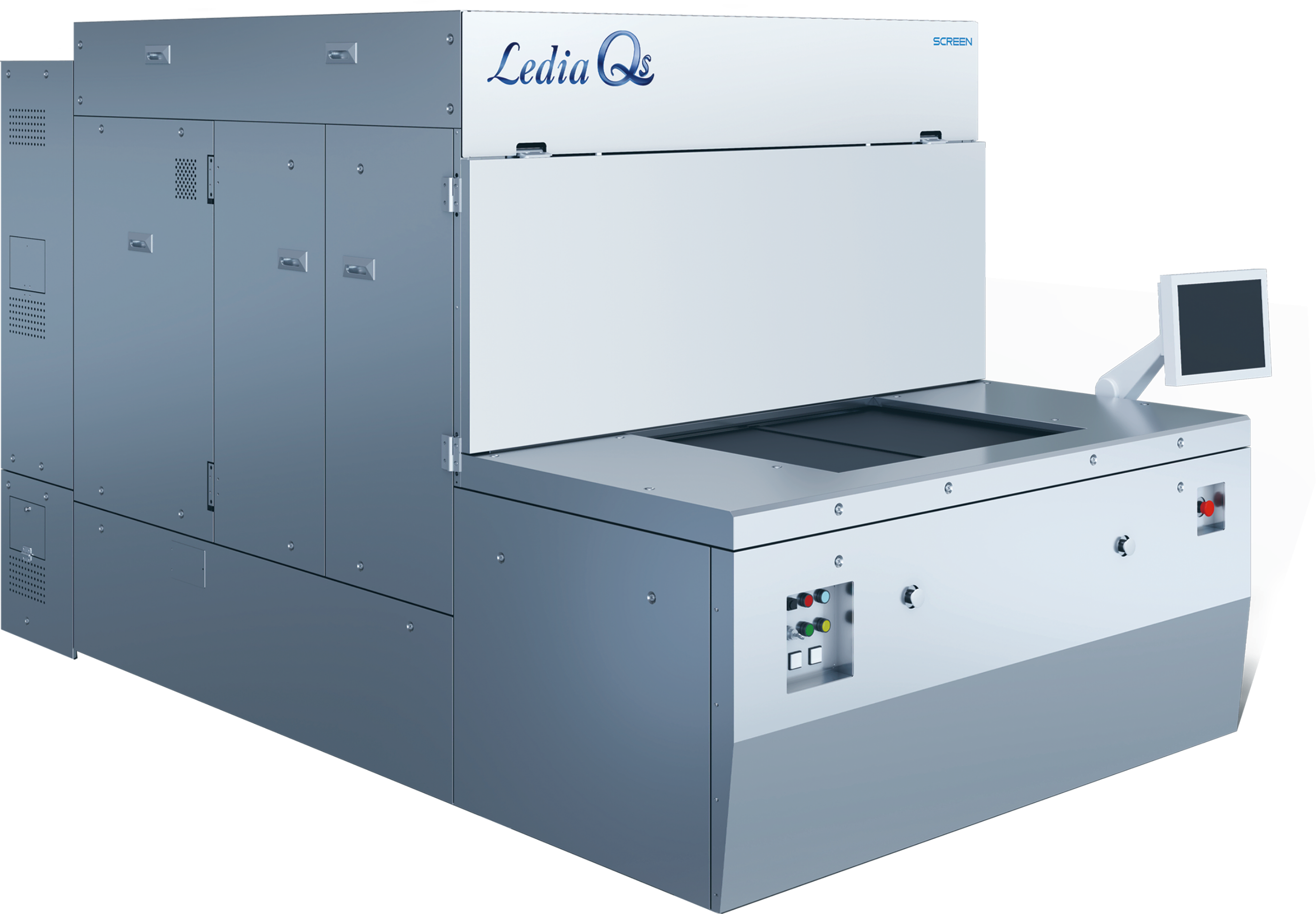
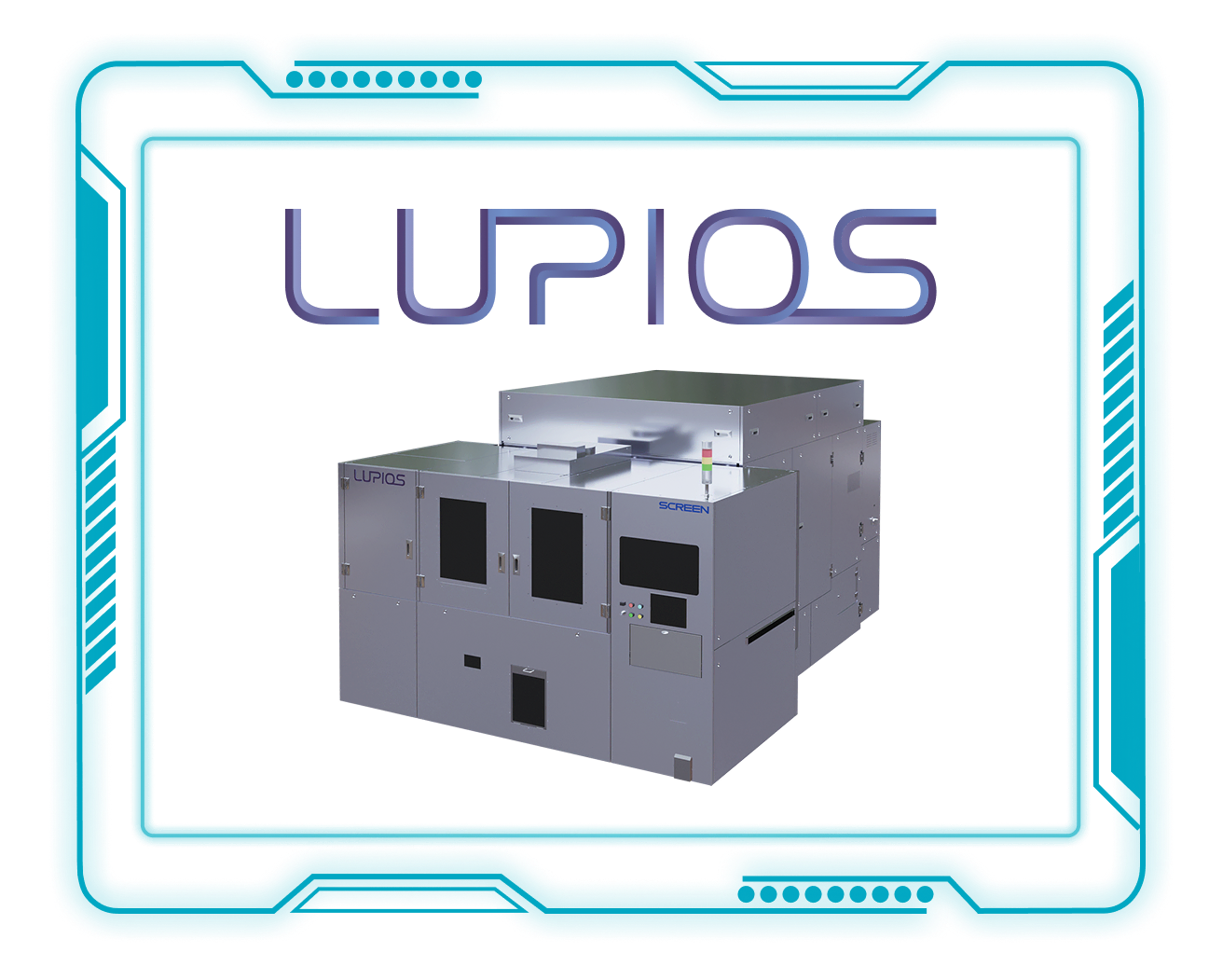
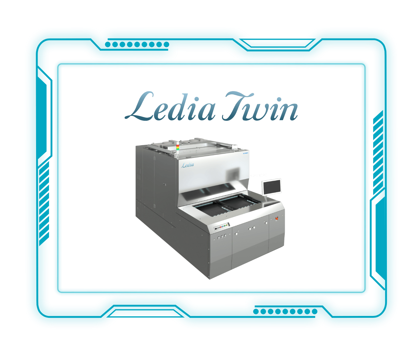
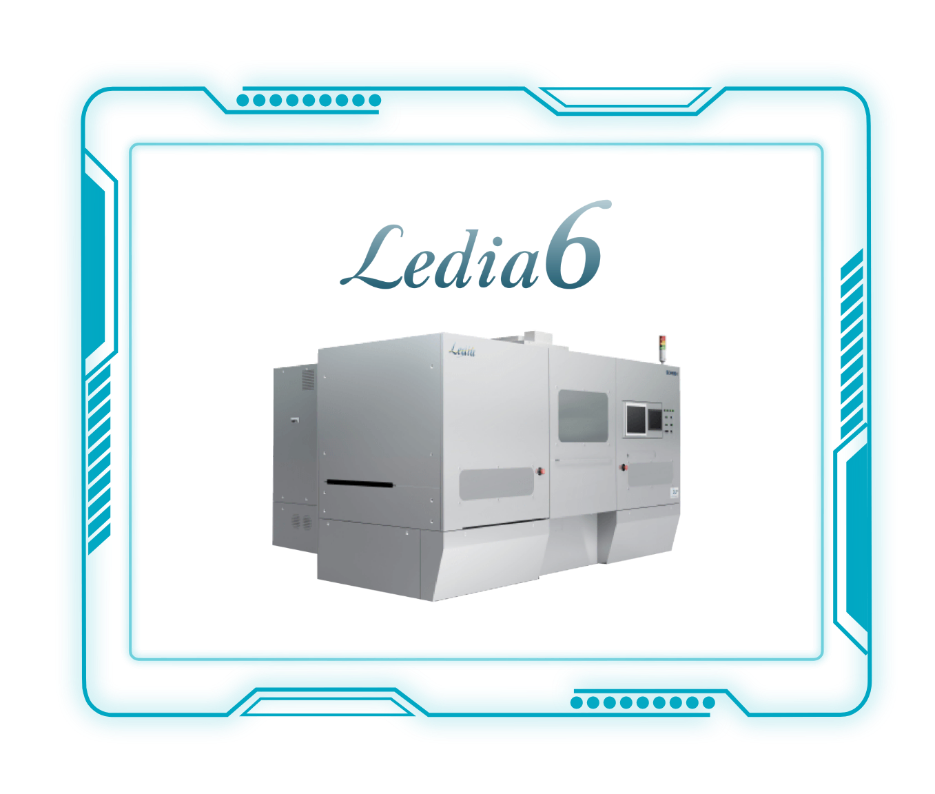
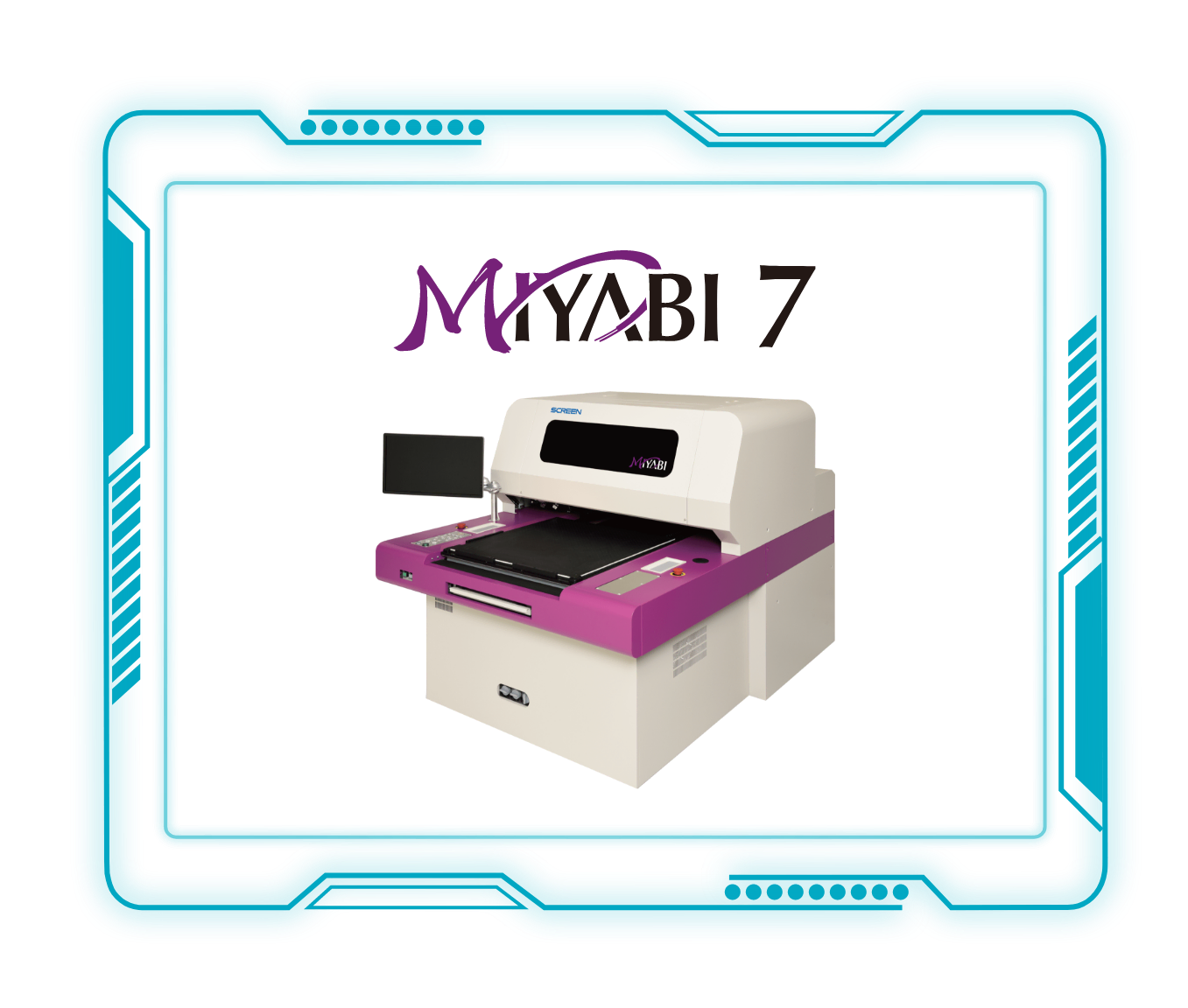
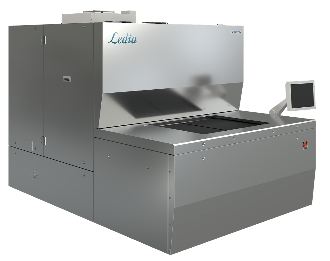
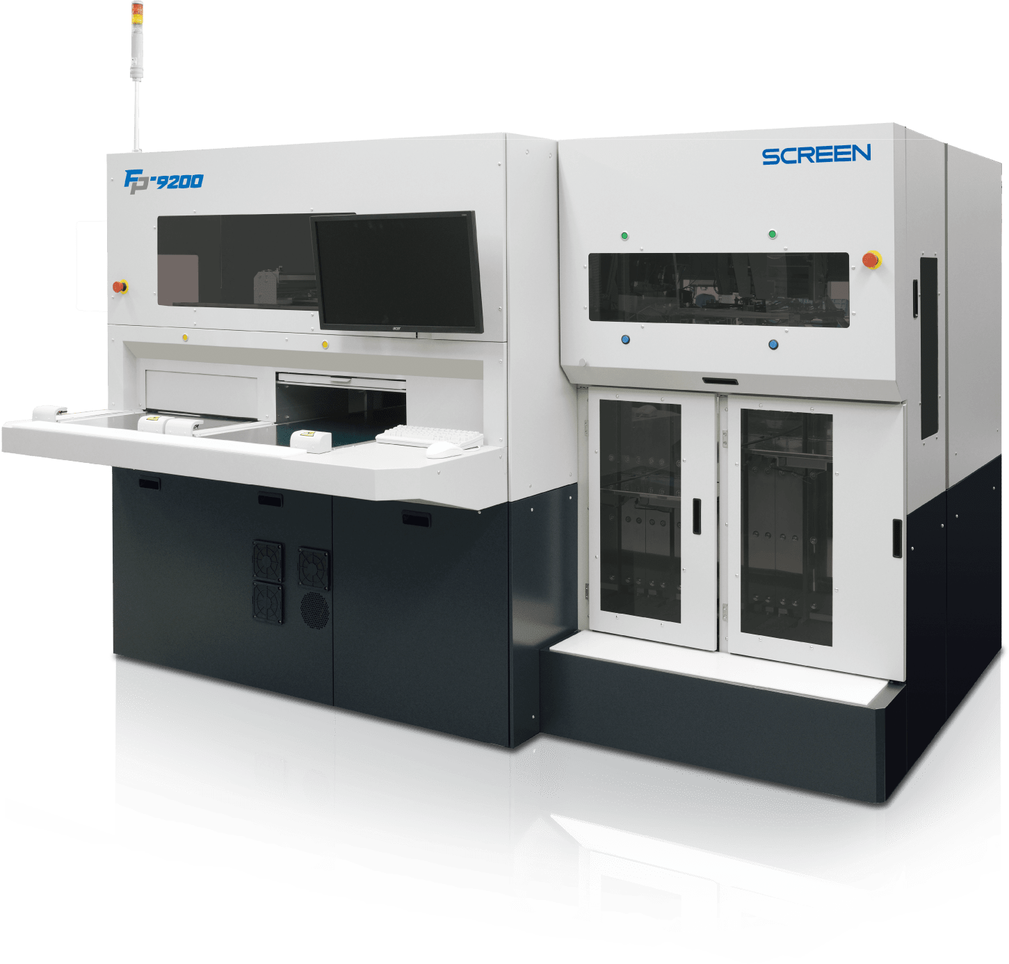
Direct Imaging System

The most ideal direct imaging equipment for various semiconductor package substrates by starting with FC-CSP
View more
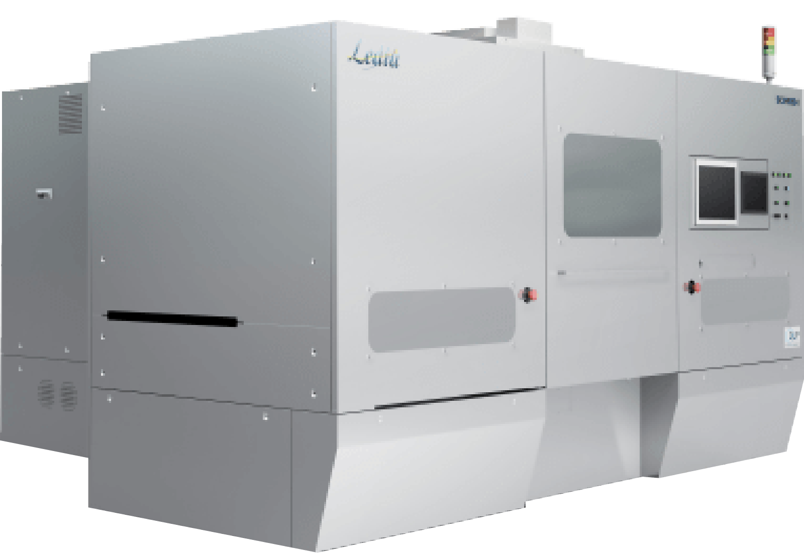
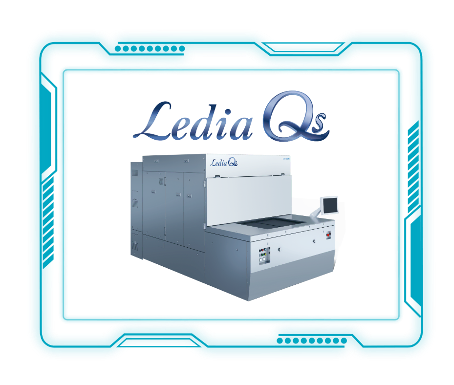
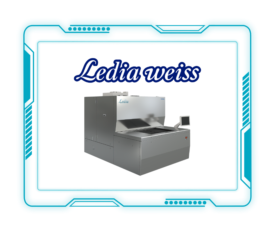
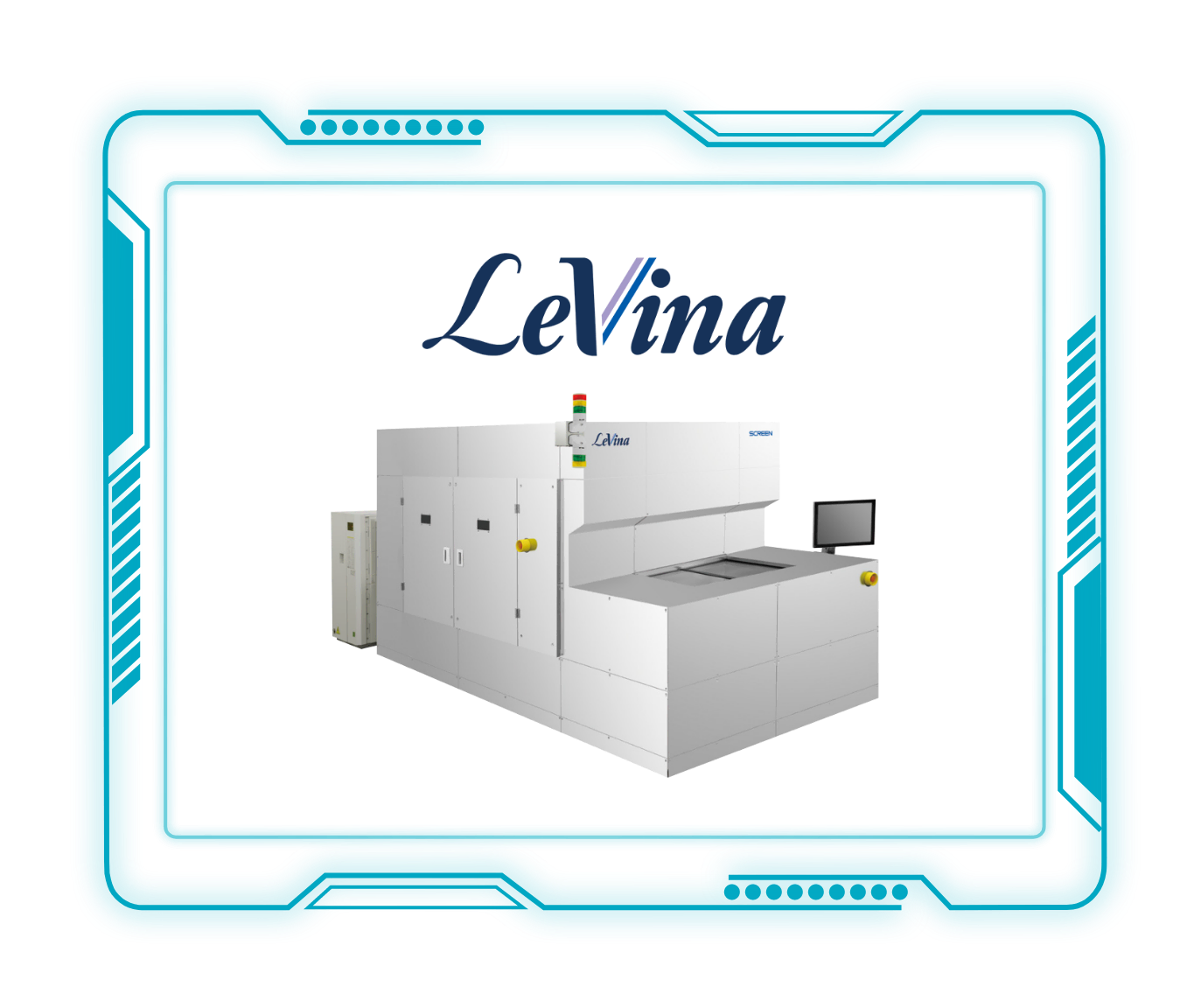
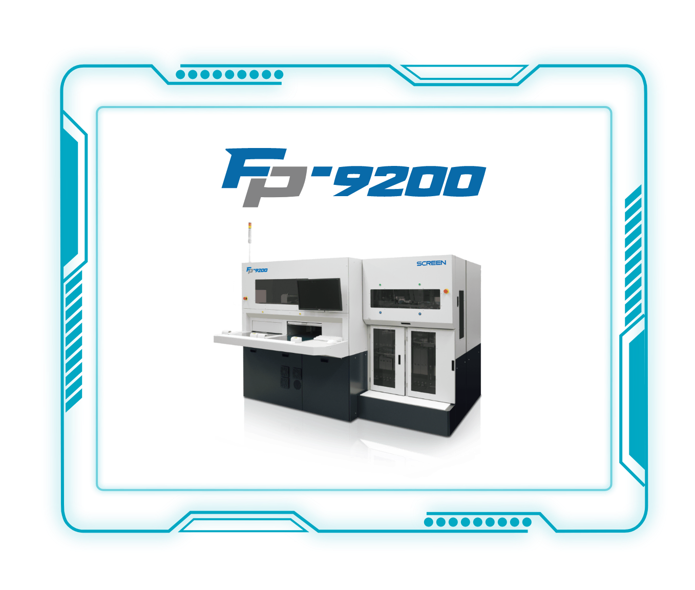
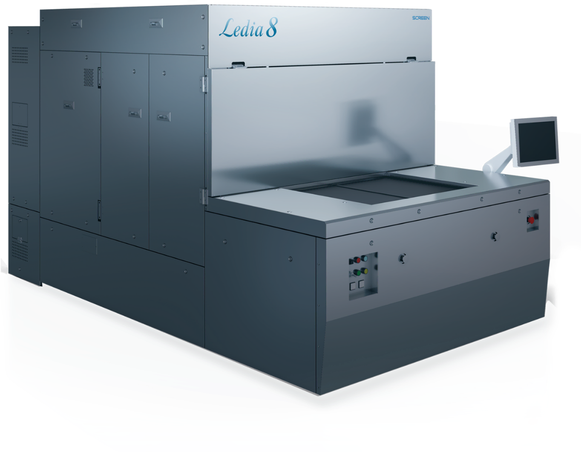
Direct Imaging System

Direct imaging equipment for patterning suitable for advanced package such as FCCSP, FCBGA and FOPLP
View more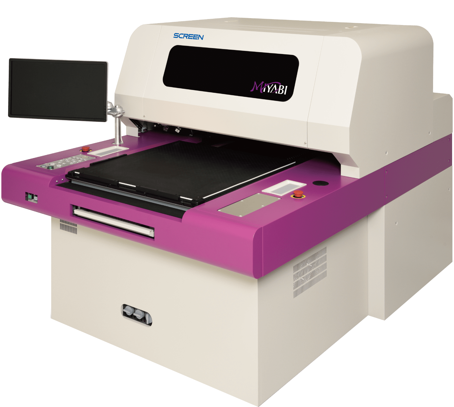
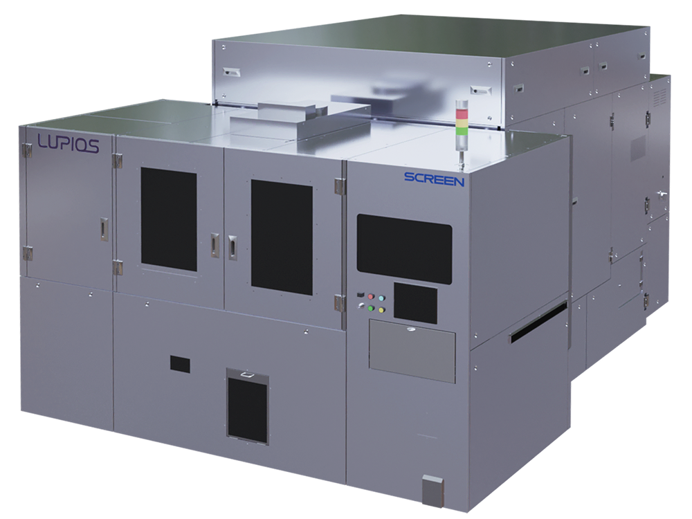
Automatic Final Visual Inspection System

Creating an optimal AVI environment with easier operation and faster verification
View more